What Can DeePMD Do too? | AI Reveals the Secret of “High-Temperature Sweating” on Silicon Surfaces
You may not know this: a silicon wafer that looks perfectly smooth is, at the atomic scale, actually a dynamic stage—silicon atoms pair up into dimers, hydrogen atoms shuttle back and forth, and at high temperatures the surface even “pre-melts,” forming a quasi-liquid layer that resembles sweating. These microscopic behaviors directly affect the quality of chip manufacturing.
Recently, the research team led by Professor Li Pai and Professor Wei Xing from the Shanghai Institute of Microsystem and Information Technology, Chinese Academy of Sciences, published a study in Small. For the first time, they systematically revealed how the Si(001) surface evolves under different temperatures and hydrogen environments, and captured its pre-melting phenomenon before bulk melting occurs. All of this relies on a key tool: Deep Potential (DP).
Why is the Silicon Surface So “Changeable”?
Silicon is the “foundation” of chips, and the Si(001) facet—due to its well-ordered structure and controllability—is widely used in semiconductor processes. But its surface is far from static: when bare, silicon atoms pair to form dimers; when hydrogen is introduced, hydrogen atoms attach to the surface, altering atomic arrangements and even triggering etching.
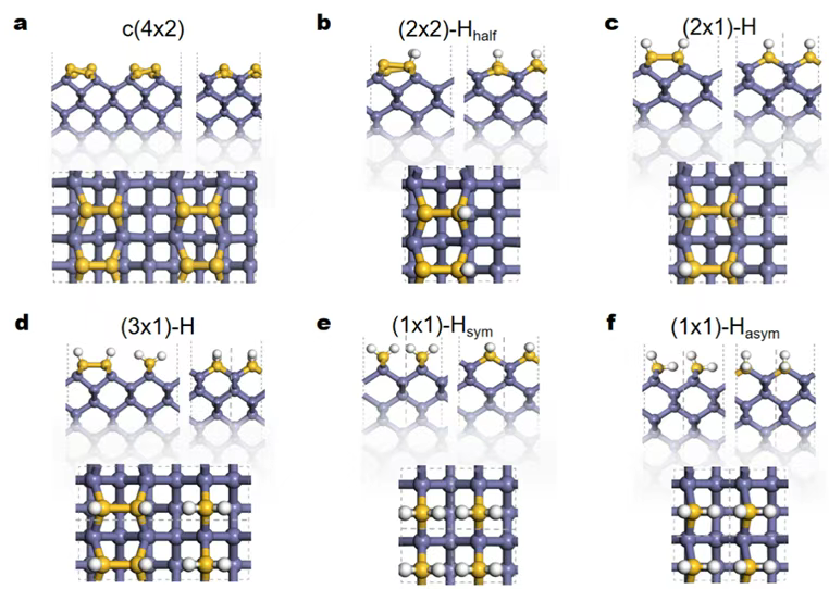
Multiple hydrogenated structures—such as (2×1)-H and (3×1)-H—have long been observed experimentally. However, a unifying theoretical explanation has been lacking:
Under what conditions does each structure appear? How do temperature and hydrogen pressure affect surface stability?
Traditional first-principles methods (like DFT) are highly accurate but extremely expensive when simulating hundreds or thousands of atoms, especially for long-time dynamics at high temperatures. This is where DP becomes indispensable.
DP: Teaching AI Quantum Mechanics—Fast and Accurate
The researchers trained a DP machine-learning force field (MLFF) using DFT data, enabling it to “learn” interatomic interactions. Once trained, the DP model achieves DFT-level accuracy while improving computational speed by several orders of magnitude—meaning problems that were previously intractable can now be simulated with ease.
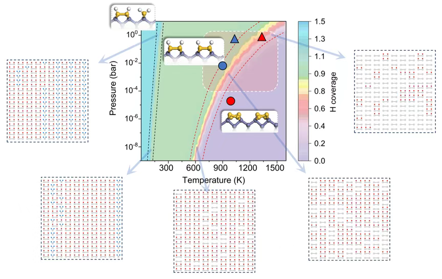
Using DP combined with grand canonical Monte Carlo (GCMC), the team constructed the first temperature–hydrogen-pressure phase diagram of the Si(001) surface. The diagram clearly reveals how surface structures evolve with environmental conditions:
- Low temperature + moderate hydrogen pressure → (3×1)-H dominated
- High temperature + high hydrogen pressure → fully hydrogenated, stable (2×1)-H phase
- High temperature + low hydrogen pressure → full hydrogen desorption, returning to the bare c(4×2) dimer structure
This phase diagram not only explains long-standing experimental observations but also highlights typical process windows used in chip manufacturing (pink box in Figure 2), providing practical guidance for industry.
Silicon “Sweats” Too? DP Reveals the Truth Behind Surface Pre-Melting
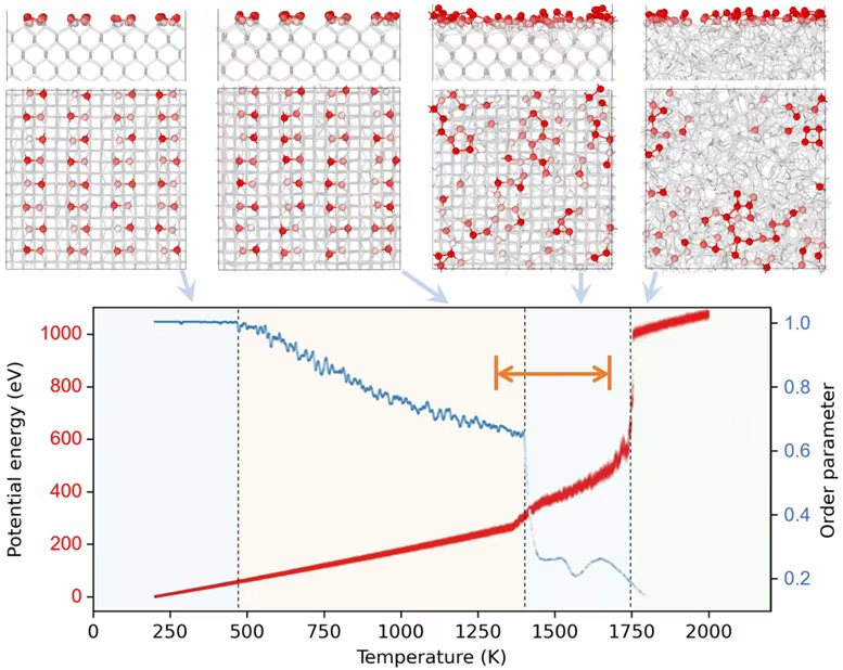
Even more strikingly, the team used DP to perform high-temperature molecular dynamics simulations of a bare Si surface (with over a thousand atoms and nanosecond timescales). They found that:
At around 1400 K (≈1127°C), although the silicon bulk has not melted (melting point ≈1687 K), the surface already begins to soften—dimers dissociate, atoms move freely in-plane, and a liquid-like quasi-molten layer forms. This “surface melts before the bulk” behavior is known as premelting.
Just like ice can exhibit a thin wet layer slightly below 0°C, premelting is a “warm-up” stage before full melting.
The DP-predicted premelting range (1300–1687 K) agrees well with experiments, and the latent heat (0.19 eV/atom) also matches experimental values (bulk ≈0.46 eV/atom). This work provides the first atomistic-resolution description of the Si surface premelting process—simulations that not only calculate, but visually “show” the phenomenon.
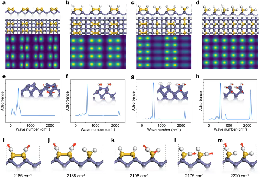
To facilitate experimental validation, the team also generated DP-based simulated scanning tunneling microscopy (STM) images and infrared (IR) spectra for different hydrogenated phases. For example:
- The Si–H stretching mode of the (2×1)-H phase appears at 2185 cm⁻¹
- The (3×1)-H phase produces a double peak around 2198 cm⁻¹
- The fully hydrogenated (1×1)-H phase shifts further to 2220 cm⁻¹
These “fingerprint signals” match experimental spectra almost perfectly, effectively providing a structural identification handbook.
Summary: DP Is Redefining the Limits of Materials Simulation
This work again demonstrates that DP is not only an accelerator, but also an explorer:
- It enables thermodynamic sampling of complex surfaces.
- It uncovers atomic-scale evolution processes that are difficult to observe experimentally.
- It bridges theory and experiment, providing atomistic insights for semiconductor manufacturing.
In the future, this approach will extend to Si(111), Si(110), and beyond, as well as more complex scenarios such as heterogeneous interfaces and defect dynamics. DP is becoming an indispensable “digital microscope” for next-generation materials research.